R&D Altanova and Essai products have been integrated into a new product unit called Advantest Interconnect Solutions™ (AIS), focusing on PCBs, sockets, and interconnect solutions. In order to streamline operations and align with the broader Advantest team, these products are now available as part of a larger ecosystem. Our joint vision is to be the premier global provider of advanced interconnect solutions. Our mission is to enable customers to achieve world-class time-to-market through our industry-leading cycle times. We prioritize safety, employee empowerment, innovation, exceptional service, integrity, continuous improvement, and environmental stewardship.
Advantest Interconnect Solutions™ (AIS) provides comprehensive, high-performance interconnect solutions tailored to meet your needs. Our experienced team of engineers collaborates closely with customers throughout the entire process, from design to manufacturing. We aim to simplify development and deliver custom end solutions that are reliable, accurate, and cost-efficient.
-
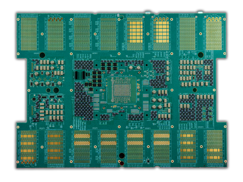
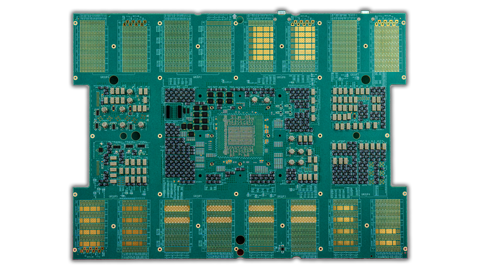
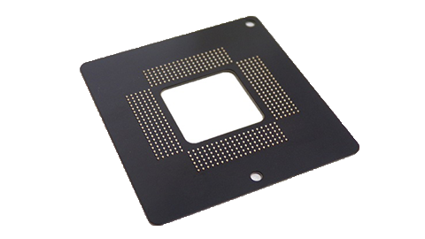
Test Interface Boards
These printed circuit boards connect test systems and sockets. They are developed and provided as part of the Advantest Interconnect Solutions™ ecosystem.
-
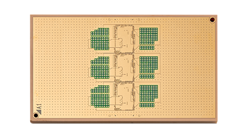
Substrates
Substrates provide the link between test boards and probe heads for Wafer Test.
-
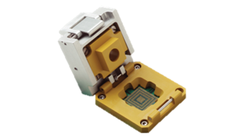
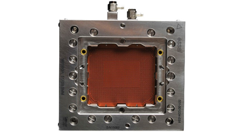
Test Sockets
Developed and provided by Advantest, test sockets mount semiconductor devices during test.
-
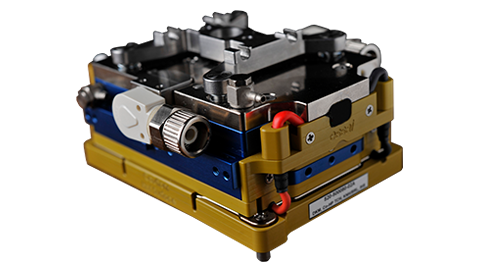
Thermal Control Units
Thermal control units precisely regulate the temperature of sockets and devices under test.
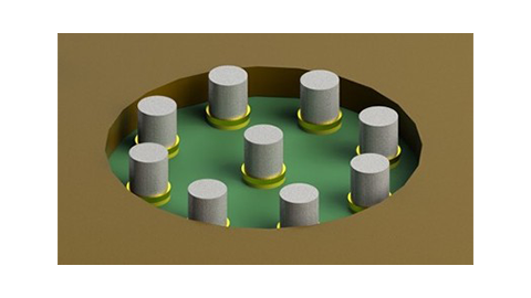
Invisipin® Series
This is a product family of device interface solutions with high precision, low loss, and excellent cost performance, developed and provided as part of the Advantest Interconnect Solutions™ ecosystem.
-
Invisipin® Solderable
First solderable elastomer pin with high performance, full reliability, and limitless configurability.
-
Invisipin® Board to Board Interconnect
Reliable, versatile, and high-speed connectivity for digital, power, and RF.
-
Invisipin® Test Sockets
High-precision, durable, and customizable for reliable, advanced testing.