Advantest Interconnect Solutions™
The Advantest Interconnect Solutions™ product unit provides test interface solutions for wafer sort and final test applications. We offer cutting-edge design, fabrication, load board PCBs, and MLO substrates. Our clients include top integrated device manufacturers, fabless semiconductor companies, and foundries worldwide.
As part of a series of strategic acquisitions, Advantest acquired Essai in 2020 and R&D Altanova in 2021, expanding its product portfolio to include leading-edge test interface boards, substrates, interconnects, test sockets, and thermal control units. As part of the company’s mid- to long-term growth strategy, the acquisitions of Essai and R&D Altanova enabled Advantest to expand its test and measurement solutions across the continuously evolving semiconductor value chain.
Quality is our top priority. We are committed to delivering high-quality products and services on time by doing it right the first time: building quality into our processes and implementing root-cause solutions to anticipate and address potential problems.
Engineering for Signal- (SI) and Power Integrity (PI)
Signal- and Power integrity (SI) is crucial in maintaining the quality of electrical signals in digital electronics, as these signals are subject to noise, distortion, and loss. Our experienced team offers comprehensive signal integrity engineering solutions, ensuring reliable performance in your Advanced Test Equipment (ATE) interface board designs.
Our services include real-world, practical design solutions, taking into account cost and performance trade-offs. We have several decades of experience in Signal- and Power Integrity modeling, instruction, measurement, and debugging, with expertise in multiple tester platforms.
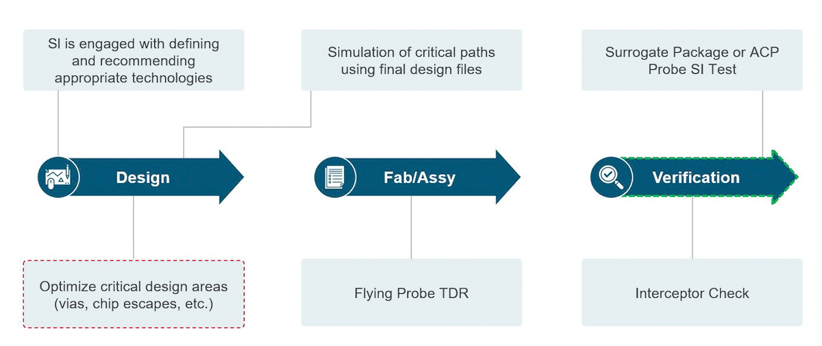
Our approach involves working closely with our customers to determine critical test requirements and recommend the best solutions from our suite of test board fabrication technologies. We simulate critical paths, optimize signal response, and verify and validate designs using advanced modeling and measurement tools.
Our resources include 3D and 2½D modeling, thermal modeling, and measurement labs capable of handling up to 50 GHz. With these solutions, our customers can be confident that their signal integrity concerns will be addressed effectively, resulting in robust and reliable designs for their test floor.
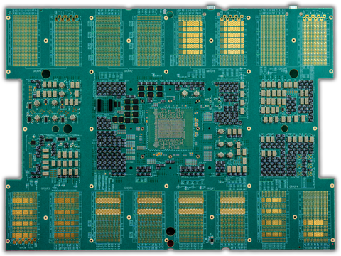
Board Manufacturing
We excel in manufacturing high aspect ratio boards, with proven capabilities of achieving aspect ratios up to 35:1 and beyond. Our facilities are equipped with high-speed drilling machines, X-ray drilling, and laser drilling and routing, ensuring precision and quality in our products. As a result, the expertise of our highly skilled engineering team ensures optimal manufacturing yields and competitive pricing.
Our integrated SI/PI engineering and design teams offer a unique advantage as they possess in-depth knowledge of our fabrication facility’s capabilities. This enables us to create tailored solutions for our customers’ test needs, addressing issues such as stack-ups, material choices, and drilling capabilities.
We continuously improve signal performance by adjusting the anti-pad in plane layers and strategically placing ground vias. For higher-speed applications, we utilize embedded coaxial vias for a significantly better signal response.
To enhance power delivery performance, we offer our EC Technology™, embedding passive components such as capacitors and resistors directly in the PWB at critical locations. This approach improves response time and allows for termination at the pin location, saving valuable surface space.
Hybrid Lamination Technology is available across different materials to match your performance and cost requirements. Performance sensitive traces are routed on selected layers, most other traces as control and power are implemented with standard technology.
Assembly and Test
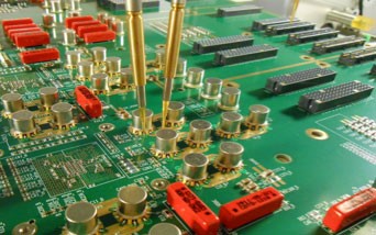
The assembly of an ATE interface board involves attaching a variety of electronic components using both through-hole and Surface-Mount Technology (SMT). Components are electrically and mechanically fixed to the board with molten metal solder using various soldering techniques. Combining both methods provides the necessary strength for components under physical stress while saving space for untouched components.
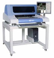
Post-assembly, the populated board undergoes multiple testing stages. First, an Automated Optical Inspection (AOI) is performed to visually check component placement, soldering quality, and adherence to JEDEC guidelines. To test the board and components electrically, we utilizes the Interceptor Test system (IT) to verify the network's functionality and create a signature for future reference after repairs. Trust our comprehensive assembly and testing process to deliver high-quality, reliable interface boards.