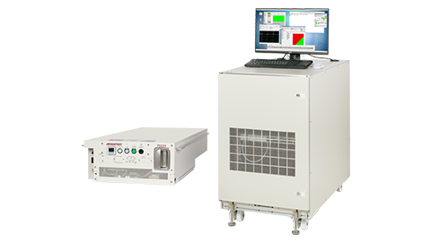
The T5221 incorporates up to 12 test stations within a third-party multi-wafer prober, each with independent testing capabilities. This delivers the best floorspace efficiency for a
non-volatile memory test system in Advantest’s history, without the need for additional footprint other than for the system controller. The tester’s massive parallelism allows it to
perform wafer-level testing on up to 1,152 devices at once, improving throughput.
As the capacity of 3D NAND devices increases, increased amounts of data output as test results have become harder to contend with. To offset the effects of these increases in data
processing time, the T5221 delivers higher data transfer speeds. As a result, test times can be further shortened and throughput is improved over previous products.
The T5221 uses Future Suite, an operating system for memory test systems that has a proven track record as the global standard. High compatibility with older systems provides users
with a seamless transition from previous generations of equipment.