
Basics of Semiconductor Wafers and Wafer Inspection
As the complexity and performance of semiconductor devices increase, higher levels of reliability than ever before are required. In this context, inspections are becoming a more important part of semiconductor manufacturing with each passing year. In particular, wafer inspections, which are performed throughout device fabrication, play a crucial role in ensuring quality, yield, and productivity. Consequently, wafer inspection equipment is in the spotlight.
This article provides a systematic overview of wafer inspection, covering everything from fundamentals, such as the purpose of inspection, types of equipment, and what is inspected at various stages of the device fabrication, to the latest trends in wafer inspection technology.
What is Silicon Wafer?
A wafer is a thin, flat round disc that serves as the substrate or base for semiconductor devices. The wafer is most commonly made of silicon (Si), depending on the applications, the wafer can also be made up of gallium arsenide (GaAs), silicon carbide (SiC), and gallium nitride (GaN).Wafers made of silicon are called silicon wafers, and when we say "semiconductor wafers," we are usually referring to silicon wafers.
Any flaws or impurities in the silicon would seriously impact the performance of the semiconductor devices made from it. Therefore, the silicon used in semiconductor manufacturing must be ultra-pure, with flaws eliminated to the maximum extent possible. For this reason, semiconductor-grade silicon is manufactured to an extremely high purity of 99.999999999% (eleven nines).
Wafers manufactured from ultra-pure silicon are supplied in standardized sizes depending on their application and manufacturing process. Common wafer diameters range from 100 mm (4 inches) to 300 mm (12 inches), with thickness typically between 0.5 mm and 1 mm.
In today's semiconductor industry, 300 mm wafers have become the standard for high-performance computing devices, while 200 mm wafers continue to play an important role in applications such as power semiconductors, automotive electronics, and industrial equipment. As a result, highly accurate inspection technologies capable of handling wafers of various sizes and applications are increasingly required.
The Role of Wafer Inspection
Wafer inspection plays a critical role in detecting defects early in the device fabrication process and preventing their downstream propagation. This reduces wasteful processing and rework, boosting yields while lowering manufacturing costs. As a result, it improves manufacturing efficiency and contributes to higher profitability. Furthermore, by strengthening quality control across the entire device fabrication process, it helps ensure the quality and reliability of the final product.
We can thus see that wafer inspection plays a vital role in semiconductor manufacturing both technically and economically.
Wafer Inspection Equipment Categories and Methods
Wafer inspection equipment is categorized by inspection target and inspection purpose. Here are some representative types of equipment:
Materials Analysis and Characterization Systems
These systems characterize the properties of the wafer material. By measuring and observing the arrangement of silicon crystals, the presence of any defects, the composition, and the internal structure of the material, they verify whether semiconductor devices made from this wafer material would operate stably.
This equipment plays a particularly important role during new material R&D and manufacturing process ramps.
Defect and Particle Inspection Systems (Optical Inspection Systems)
These systems detect defects and foreign particles by irradiating the wafer surface with light or an electron beam (E-beam) and observing differences in the intensity or spread of the reflected signals.
Optical systems, which utilize laser or broadband light sources, perform inspections based on differences in reflected or scattered light. They operate at high speed, making them suitable for in-line inspection during mass production. In contrast, E-beam systems form images by detecting secondary or backscattered electrons emitted from the wafer surface when it is scanned with a focused electron beam and analyze these images to identify structural variations or the presence of defects. Because electrons have a much shorter effective wavelength than light, this method enables high-resolution detection at the nanometer level, which can identify tiny structural irregularities or defects that are difficult for optical systems to capture.
The choice of inspection method depends on the stage of the device fabrication process where it is used, as the specific role of the equipment and key inspection priorities vary accordingly. In particular, the goal of inspection differs significantly depending on whether the target is a bare wafer, with no circuits on it yet, or one that has already been patterned.
Inspections of bare wafers prior to patterning focus on detecting surface flatness issues, the presence of foreign particles, and visual anomalies such as scratches. This enables assessments of process integrity aimed at identifying exactly which piece of equipment or process step caused the scratching or contamination, thus facilitating improvements to process conditions and equipment.
Conversely, inspections of wafers that have already been patterned with transistors and wiring circuits detect visual anomalies such as adhered foreign particles or circuit shapes that deviate from design specifications.
Dimension and Profile Metrology Systems
Dimension and profile metrology systems are used to precisely measure parameters such as circuit
pattern linewidths (critical dimensions), shapes, film thicknesses, and wafer warpage. A good
example is CD-SEM (Critical Dimension Scanning Electron Microscope) tools, which utilize scanning
electron microscope technology. They use an electron beam to measure circuit pattern dimensions and
shapes with nanometer-level precision based on the backscattered electrons from the wafer.
The
measurement data is fed back into the device fabrication process, playing a vital role in preventing
yield degradation through early defect detection and process control.
Key Semiconductor Wafer Inspection Processes
Semiconductor manufacturing processes are broadly divided into front-end processes, where circuits are fabricated on wafers, and back-end processes, which include assembly, packaging, and final test. Wafer inspection is primarily conducted at the front end and includes optical review, critical dimension measurement, defect inspection, and electrical test.
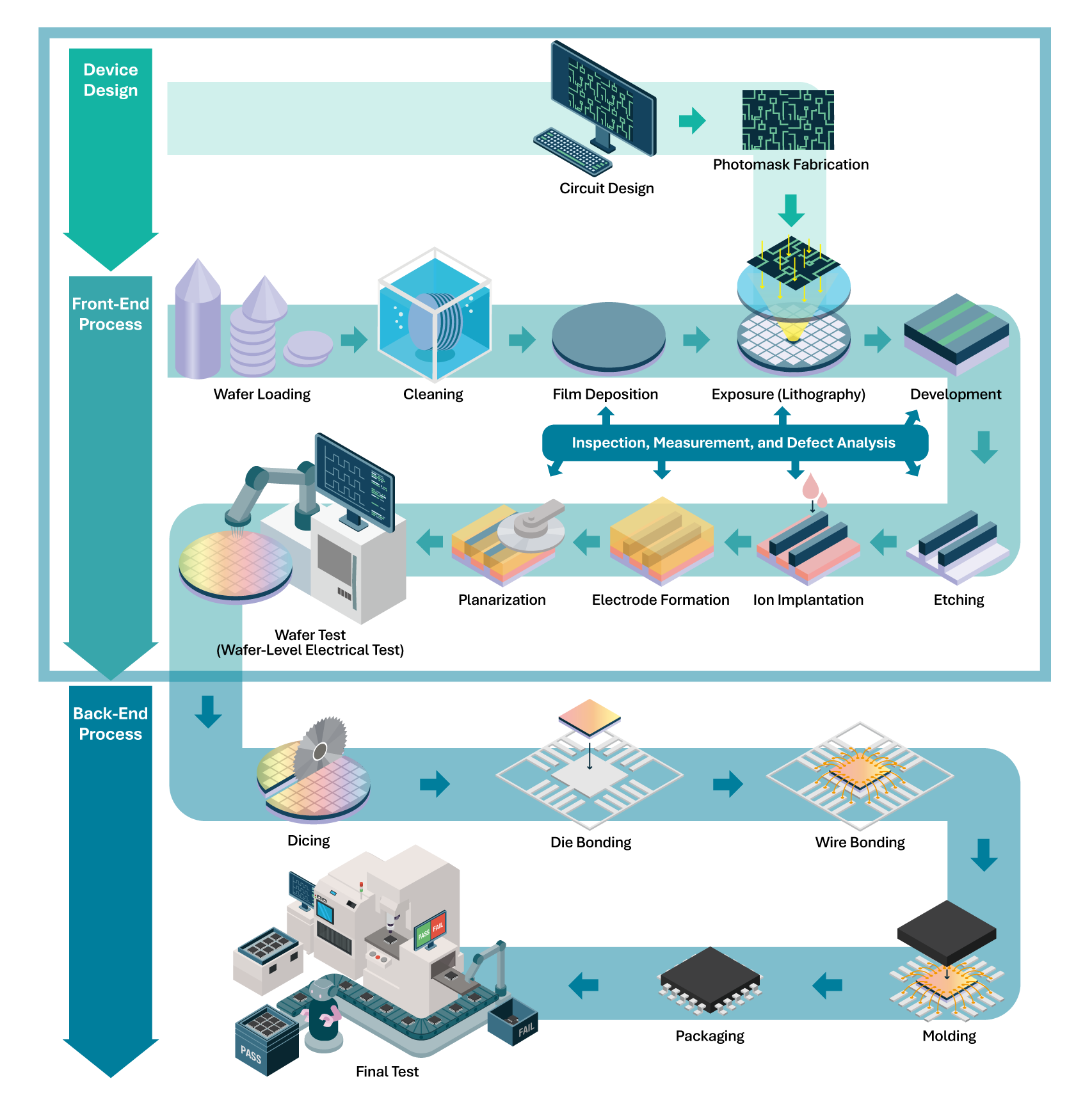
Review, Critical Dimension Measurement, and Defect Inspection
During the front-end processes where semiconductor chip circuits and elements are fabricated on a wafer, optical review, critical dimension (CD) measurement, and defect inspection are performed to verify that circuit patterns match design specifications. A typical inspection method used for this purpose is CD-SEM (Critical Dimension Scanning Electron Microscopy), which allows for the detailed examination of circuit pattern dimensions and shapes at the nanometer scale.
This enables early detection of critical dimension variations, microscopic defects, and particles. Analyzing the acquired data also makes it possible to identify process abnormalities.
Wafer-Level Electrical Test
Electrical test processes are used to verify that circuits fabricated on a wafer operate correctly from an electrical standpoint.
In the context of wafer inspection, wafer-level electrical test is a process that evaluates the electrical characteristics of semiconductors before the wafer is diced into individual dies. A tester and a wafer prober are used to confirm that the electrical characteristics of the circuits conform to design specifications and function correctly.
A wafer prober is a tool that establishes an electrical connection by contacting the electrodes of the chips on the wafer with needle-like probes, enabling the tester to measure electrical signals.
So, while CD-SEM and other tools are used to measure the critical dimensions of semiconductors and inspect them for defects at the wafer level, electrical test evaluates semiconductors from a different perspective by measuring the operational characteristics and electrical performance of their circuits.
Thus, we can see that semiconductor quality assurance relies on a variety of inspection and measurement methods.
For more information on semiconductor test equipment (ATE), please check this article.
Back-End Inspection & Final Test
After the inspection processes described above, the wafers are diced into individual dies, each with integrated circuitry formed on it, and the dies are then packaged. This is the back-end process, where the dies take their final form as semiconductor devices. Various tests are conducted as a final verification step to ensure product quality and reliability.
Specifically, wire bond inspection is performed to verify that the wires that connect the semiconductor chip to external circuitry are securely and correctly attached. Next, optical inspection uses high-resolution cameras and image processing to detect minute scratches, cracks, or deformations on the packaged semiconductor devices. Lastly, automatic test equipment (ATE) performs a final electrical test to measure and evaluate performance, functionality, and reliability.
Wafer Inspection Technological Trends & Outlook
The wafer inspection technologies explained above continue to evolve in step with the increasing sophistication of manufacturing processes.
In particular, the future of inspection technology cannot be discussed without mentioning artificial intelligence (AI) and other technologies needed to ensure the quality of next-generation devices.
AI Improves Accuracy of Wafer Inspection
AI—specifically, image recognition technology utilizing deep learning-is already being employed in optical wafer inspection. In addition to enabling automated defect detection and more accurate defect classification, it is also expected to reduce false positives.
False positives are anomalies identified as defects by inspection equipment that do not impact electrical characteristics or reliability. They do not actually mean the wafer needs to be discarded.
Because AI can be trained on the judgment and know-how of skilled experts, it offers significant advantages in terms of distinguishing between false positives and actual defects.
EUV Lithography Requires Better Mask Inspection Technology
Semiconductor circuit patterns are formed on wafers by lithography, a process where patterns are transferred from a mask, a master plate that serves as a blueprint for the circuit pattern, onto the photoresist layer of a wafer.
As semiconductor features shrink, lithography technology must support the accurate transfer of finer and tinier patterns. Since pattern resolution depends on the wavelength of the light used by the lithography system, using shorter wavelengths enables finer-scale fabrication.
Consequently, semiconductor manufacturers have recently adopted EUV (Extreme Ultraviolet) lithography, which utilizes shorter wavelengths to achieve higher resolution.
This means that tiny defects on the mask, previously not a problem, are now more likely to be accidentally transferred onto the wafer, resulting in circuit failures. Furthermore, because a single mask can transfer its defects onto numerous wafers, it can have a devastating impact on production yield.
To avoid this outcome, semiconductor manufacturers perform mask inspection throughout the entire process, from mask manufacturing to quality evaluation.
Advanced inspection and review systems help identify pattern defects, contaminants, and other anomalies before they are transferred onto wafers.
As a result, the ability to reliably detect and eliminate tiny defects at the mask level has become increasingly important. The importance of technologies for detecting and evaluating such microscopic defects is expected to grow significantly in the future.
The Increasing Importance of Die-Level Test
A notable development in recent years is advances in chiplet technology where multiple dies, each with specific functions, are combined within a single package to form a single device, instead of integrating all these functions onto a single large semiconductor chip.
Chiplet design enables higher performance and flexible customization of functions, but it also makes quality assurance for individual dies even more important.
Thus, not only wafer-level inspection but also die-level testing, which is performed on individual dies after they have been diced, is becoming increasingly important, particularly for advanced packaging and chiplet-based devices where the quality of each die directly affects the performance of the final product.
Demand for electrical test and optical inspection at the die level is therefore growing, along with the need for increasingly sophisticated handling technologies capable of manipulating tiny, fragile dies with high precision. Handlers-which work with testers to transport and precisely position the dies for test-are expected to play an increasingly vital role as the core technology supporting these advancements.
Advantest's Wafer & Mask Inspection Portfolio
Advantest provides wafer and mask inspection solutions that leverage scanning electron microscope technology.
-
CD-SEM: These systems measure the critical dimensions of tiny circuit patterns on semiconductor masks with high precision.
-
Mask DR-SEM: These systems inspect and analyze tiny defects detected by wafer and mask inspection systems at very high magnification, contributing to process improvements and higher yields.
As one of the world's premier measurement technology companies, Advantest provides unmatched value in wafer and mask inspection systems and continues to support the evolution of semiconductor technology together with our customers.
Supervised by
Advantest Content Editorial Team
* The information provided is current as of October 13, 2026.