
In today's digital society, semiconductors are used everywhere. The adoption of artificial intelligence (AI), improvements in smartphone performance, and applications such as automobiles and medical devices, as well as the expansion of data centers, illustrate how essential semiconductors have become in modern society.
No matter how innovative a semiconductor design may be, every part of the device must operate consistently and reliably for the chip to function as a whole. This is where ATE, also known as semiconductor test equipment, plays a central role.
In this article, we explain what ATE is, why it is important, how ATE systems are structured, and the challenges and future directions driven by advanced semiconductors.
What Is ATE (Automated Test Equipment)? Its Role and Importance
ATE, also known as semiconductor test equipment, is used to test whether semiconductor devices operate as intended according to their design specifications.
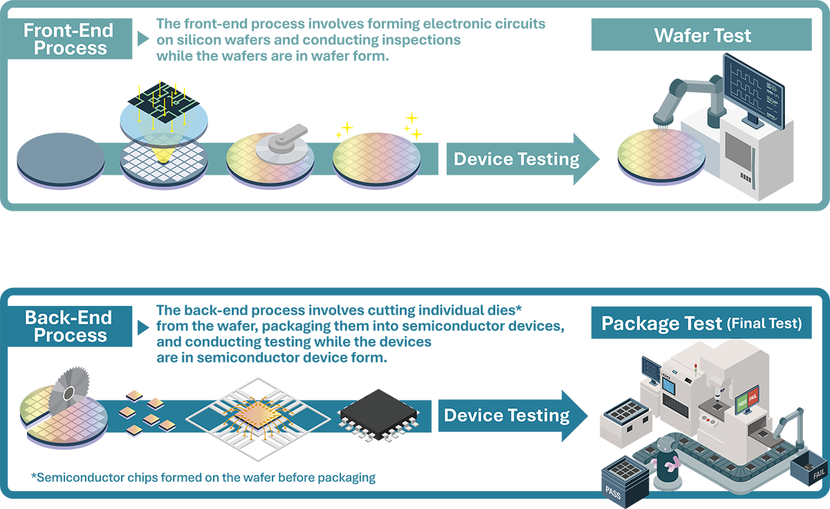
The semiconductor manufacturing process is broadly divided into two stages. The first is the front-end process, where electronic circuits are formed on silicon wafers. The second is the back-end process, where individual dies are cut from the wafer, assembled, and packaged into finished semiconductor devices. ATE is used throughout these manufacturing stages to identify potential defects and distinguish "good" die from "bad" die.
Additionally, ATE plays an important role in evaluating how semiconductors perform under conditions that simulate real-world use. By testing devices in environments that reflect actual operating conditions, ATE helps confirm that each semiconductor can deliver its intended performance and operate stably over long periods of time. In this regard, advanced test systems such as ATE are widely regarded within the industry as key tools enabling the world's most advanced semiconductors.
Why Is ATE Essential in Semiconductor Manufacturing?
Semiconductors are deeply embedded in modern society and play a critical role in the devices we rely on every day. Because of this, ensuring their quality and reliability typically requires 100% inspection and testing.
At the same time, as semiconductor device structures become more complex and production volumes continue to grow, the number of test items and the time required for testing have increased. As a result, ATE has become indispensable in semiconductor manufacturing for performing highly accurate and efficient 100% inspection.
Ensuring the reliability of semiconductors used in products such as smartphones, personal computers, and automobiles has strategic importance for manufacturers beyond simple quality control, as it directly affects profit margins and brand trust.
To better understand the role of ATE, let us compare ATE with manual testing procedures traditionally used in research and development environments.
Manual testing typically involves the following steps:
-
Environment setup (manual connection of measurement instruments)
-
Physical contact (probing fine electrodes under a microscope)
-
Test execution (measurement and recording using manual controls)
-
Verification (comparison with data sheets)
This approach is suitable for testing a single device at a time.
In contrast, ATE is designed to test multiple devices simultaneously and to automate the testing process. This reduces human error and enables stable and consistent testing. As a result, ATE delivers benefits such as improved quality and reliability, maximized production efficiency with lower costs, and shorter product development cycles.
Improving Quality and Reliability
Defects in semiconductor devices can cause significant disruption to our daily lives. For example, issues such as navigation systems malfunctioning or smartphones failing to connect can affect everyday activities. Beyond such inconveniences, semiconductors also play critical roles in applications such as medical devices and automotive safety systems, where failures can have serious consequences. In addition, modern data centers contain vast numbers of chips, and even a single malfunction can lead to large-scale disruptions and significant resource losses.
For this reason, ensuring high levels of quality and reliability is essential in semiconductor manufacturing.
How is test performed?
ATE performs meticulous testing by applying electrical signals to semiconductor devices to verify whether they operate correctly, run at a specified speed, and show no abnormal current flow. These tests are performed at each step of the manufacturing process, from wafer, die-level, packaging, and system-level.
ATE also performs “burn-in” test, in which extreme conditions such as high-temperature and high-voltage is applied to the device to reveal stress-induced defects that are more likely to appear early in the device’s lifetime, identifying faulty devices before they reach the consumer.
Reducing failure rates in the market as much as possible, while minimizing the time required to reach the target quality level, is an important step in improving product reliability.
Maximizing Production Efficiency and Reducing Costs
Improving the efficiency of the testing process directly reduces the cost per device. One of the key characteristics of ATE is its ability to test many devices at the same time. By testing multiple devices simultaneously in a single measurement, ATE significantly increases throughput, or the number of devices produced per unit of time.
Detecting defective chips early in the front-end process also has significant economic value. Applying expensive packaging and assembly processes to chips that are defective wastes valuable time and resources. By enabling early detection of defects, ATE helps eliminate waste throughout the manufacturing process. Through improved yield, it also provides value that ultimately contributes to higher profitability for customers.
Shortening the Product Development Cycle
In the development of new semiconductor devices, a great deal of time is spent on the debugging process to verify whether the device operates as designed. As devices become more advanced, the number of items that must be verified increases, making this debugging process a bottleneck in the overall development.
ATE applies simulation results from the design stage to actual devices and quickly presents test results for prototype devices. This makes it possible to confirm device behavior and proceed to the next stages of verification and analysis. By automating and accelerating these processes, ATE enables design engineers to identify issues earlier on and correct them, shortening the overall product development cycle and reducing the time required to bring products to market.
Key Components and Types of ATE Systems
ATE is a highly integrated system that combines a tester for precise signal processing, peripheral equipment that handles the semiconductor devices being tested, and software that controls and coordinates these elements.
Tester: Directing Electrical Measurements
The tester serves as the control unit of an ATE system. It applies electrical signals to a semiconductor device and compares the electrical signals returned from the device with predefined expected data.
Probers and Test Handlers: Supporting Devices for Accurate Testing
While the tester directs the measurement process, peripheral equipment such as probers and test handlers physically transports devices and supports the progress of testing. These peripheral systems move devices to designated positions within the equipment and, once the devices are properly set, signal to the tester that they are ready. After receiving this signal, the tester begins the test. When testing is complete, the tester sends a completion signal back to the peripheral equipment. Based on the test results received, the peripheral equipment sorts the devices. This sequence is automatically repeated until all devices have been tested.
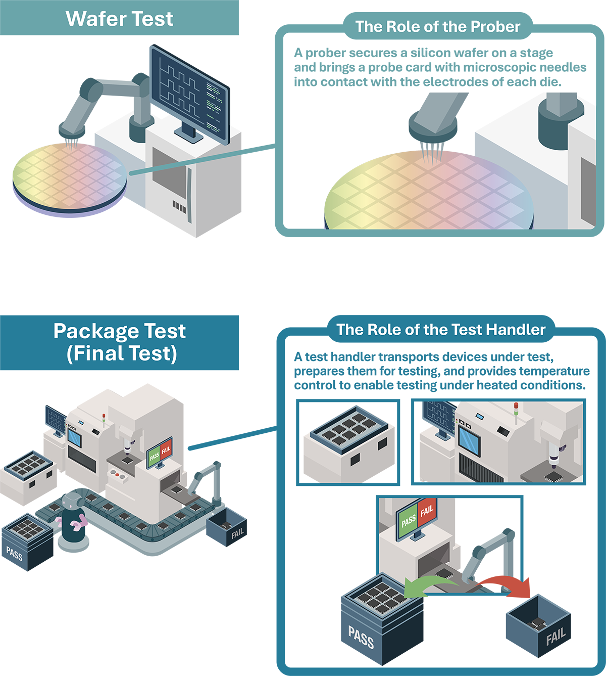
Prober
Probers are used in the wafer test stage (front-end process). They precisely secure a silicon wafer on a stage and bring a probe card containing microscopic needles into contact with the electrodes of each die (semiconductor chips formed on the wafer before packaging). This establishes an electrical connection with the tester, enabling performance testing while the devices remain in wafer form.
Test Handler
Test handlers are used in the final test stage (back-end process) after packaging. A test handler transports the devices under test and inserts them into sockets that electrically connect the devices to the tester. Test handlers are also equipped with temperature-control functions, allowing device operation to be checked under heated conditions that simulate actual usage environments.
ATE Coverage Across the Semiconductor Lifecycle
The scope of ATE is expanding to cover the entire lifecycle of semiconductor devices.
-
Design and prototype evaluation: ATE works in conjunction with Design for Testability (DFT), a technique that incorporates test-friendly features into semiconductor devices from the design stage. Simulation results are compared and analyzed alongside measurement results from actual devices. DFT refers to a method in which dedicated test circuits are embedded into a device during the design phase to enable efficient testing for defects after manufacturing.
-
Wafer-level testing: Testing is performed on silicon wafers before they are diced into individual dies. This stage verifies the electrical characteristics of each die while still on the wafer, enabling early detection of defects.
-
Die-level testing: After wafer inspection, testing is performed on individual dies that are diced from the wafer. This type of testing is carried out to secure known-good dies before packaging, particularly for advanced packaging technologies such as chiplets and 3D stacking.
-
Package testing: Package testing verifies whether packaged devices operate correctly as completed semiconductor products. In addition to checking electrical characteristics and basic functions, devices are tested to confirm stable operation under conditions such as temperature variation. Defective devices are screened out before shipment. Package testing is also referred to as final testing.
-
System-level testing (SLT): System-level testing is performed on platforms that reproduce operating conditions close to actual usage environments of final products, such as smartphones and personal computers. By running operating systems and software, SLT helps identify failures caused by complex interactions between hardware and software that are difficult to detect with test-specific programs.
Challenges and Initiatives in the ATE Industry
As semiconductor technology continues to advance, the importance of semiconductor testing is increasing. Devices for applications such as AI and high-performance computing (HPC) are becoming more complex.
These advances bring some challenges, including increased integration complexity, greater difficulty in thermal management, and strong demands to reduce defects.
To address these challenges, efforts are accelerating to fundamentally improve the efficiency of the testing process through advanced use of data and AI.
Increasing Semiconductor Complexity and Rising Test Costs
In the past, semiconductor devices were mainly monolithic, with all functions integrated onto a single silicon substrate. Today, chiplets, which combine smaller semiconductor dies (individual chips) with specific roles, and 3D integration, in which dies are stacked vertically, are becoming common in modern-day chips.
The effects of these structural changes reach beyond manufacturing. They also create challenges for testing, as conventional approaches are no longer sufficient. Specifically, we see challenges in the following three areas:
-
Increased complexity and defects due to integration: Semiconductor structures are evolving toward combining functions such as computing, communication, high-bandwidth memory, and power control within a single package—functions that were previously designed and verified separately. As a result, issues may emerge only after integration, even if each function operates correctly on its own.
-
Difficulty in thermal management: To verify performance, advanced AI devices must be operated under high loads during testing, which generates significant heat. Moreover, as chips grow smaller in size, their architectures become denser and generate more heat. Appropriate cooling is required to prevent hot spots that could damage the device.
-
Strong demand for defect reduction: For advanced devices, such as those used for generative AI, even a single defective chip can affect the entire system. As a result, extremely strict quality standards aiming for zero defective parts per million or “zero DPPM” are required.
Addressing ATE Challenges: Driving Efficiency Through AI and Data Utilization
In the semiconductor industry, methods that use the vast amounts of data generated during testing to improve both testing accuracy and efficiency are becoming more widely adopted in response to increasingly complex challenges. Advantest is also strategically promoting the automation of testing by combining test data utilization with AI technologies.
Balancing Quality and Efficiency Through Data Analytics
By building a system for centralized management of measurement data, efficiency across the entire manufacturing process is being improved.
-
Real-time data utilization: An infrastructure is used to collect and provide large volumes of data generated during test execution in real time. This makes it possible to assess conditions immediately using advanced calculations without interrupting the testing flow.
-
Adaptive testing: Based on the collected data, test flows are optimized according to the condition of each device and its position on the wafer. This contributes to shorter test times while maintaining product quality.
Accelerating Development Through the Use of Digital Twin Technology
Here, "digital twin" refers to a model that reproduces actual equipment and processes in a virtual environment based on data, enabling operation verification and optimization under conditions similar to those in the real world. To improve development efficiency, software that recreates physical testing environments in a virtual space is being deployed. This makes it possible to develop and debug test programs before devices are completed, significantly shortening the time required to achieve mass production.
Large-Scale Data Processing Using a Proprietary High-Speed Communication Network
To support large volumes of test data required by advanced AI devices, a proprietary high-speed communication technology optimized for use within the test system is employed. This enables large amounts of data to be transferred at high speed while multiple processes are executed in parallel. As a result, complex device performance can be evaluated accurately, while testing efficiency is improved by increasing the number of tests performed per unit of time.
The Future of Semiconductor Devices Enabled by ATE
This article has explained ATE (Automated Test Equipment), which supports semiconductor quality, covering its role, system structure, and recent trends. As semiconductor devices continue to become smaller and more complex, and as AI is increasingly used across many areas of society, ATE supports the essential test processes required to ensure quality and maintain the reliability of semiconductor products.
Frequently Asked Questions (FAQ) About ATE
Advantest's Evolution as a Leader in the ATE Semiconductor Field and Next-Generation ATE Solutions
Advantest has grown alongside the development of the semiconductor industry as a global leader in semiconductor testing.
The company was founded in 1954 as Takeda Riken Industry Co., Ltd., an electronic measurement instrument manufacturer. Its early products included the "Micro‑Micro Ammeter," which measured extremely small electrical currents. This precision measurement technology later became the foundation of Advantest's ATE (Automated Test Equipment) business.
In the late 1960s, anticipating the growth of the semiconductor industry, Advantest began full-scale development of ATE by applying its proprietary measurement technologies. Today, Advantest has established its position as one of the leading players in the ATE field through continuous technological innovation.
Latest Solutions Addressing Increasingly Complex Needs
As a partner contributing to the reliability of the semiconductor value chain, Advantest provides comprehensive semiconductor test solutions that meet the diverse needs of various semiconductor devices and customers. By offering solutions built on a common platform—from development-oriented systems that reduce initial investment to highly efficient systems for mass production—Advantest helps customers optimize their return on investment.
-
V93000: A high-performance SoC test system and one of Advantest's flagship testers, widely deployed in factories around the world. The latest generation, V93000 EXA Scale™, incorporates the proprietary communication network Xtreme Link™, enabling efficient and reliable processing of the rapidly increasing volumes of test data required for AI and HPC devices.
-
T2000: An open-architecture tester with a modular design. It can be flexibly reconfigured to support diverse testing needs, including microcontrollers, automotive devices, and analog devices.
-
Memory Testers: Advantest's memory testers support a wide range of processes, from wafer testing to package testing. Their ability to test many devices simultaneously, together with stable measurement performance, supports the needs of high-volume manufacturing and ensures product quality. Product families such as T5801 and T5833 address the evolving requirements of the memory market.
-
ACS (Advantest® Cloud Solutions): A platform that integrates advanced data analytics with ATE. By analyzing large volumes of data generated by ATE in real time, ACS enables adaptive testing and automated yield optimization, contributing to improved quality across manufacturing processes.
Building on its core measurement technologies, refined since its founding, Advantest will continue to take on the challenge of testing increasingly high-performance and complex semiconductors together with customers worldwide.
Supervised by
Advantest Content Editorial Team
* The information provided is current as of July 2, 2026.