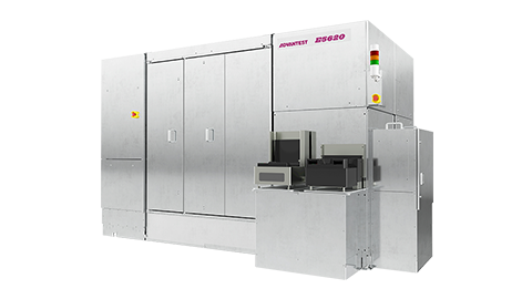
Metrology / SEM
Our SEM products use scanning electron microscope technology to measure and review tiny surface structures such as photomask etching and circuitry on wafers with high precision and stability.
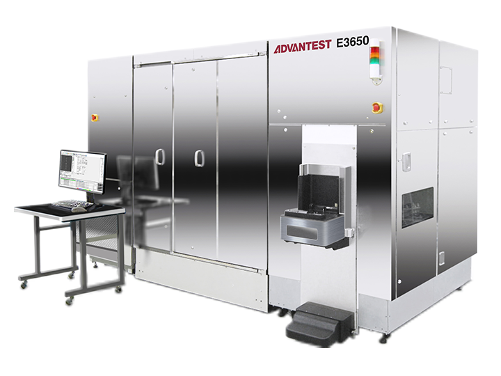
Our SEM products use scanning electron microscope technology to measure and review tiny surface structures such as photomask etching and circuitry on wafers with high precision and stability.