-
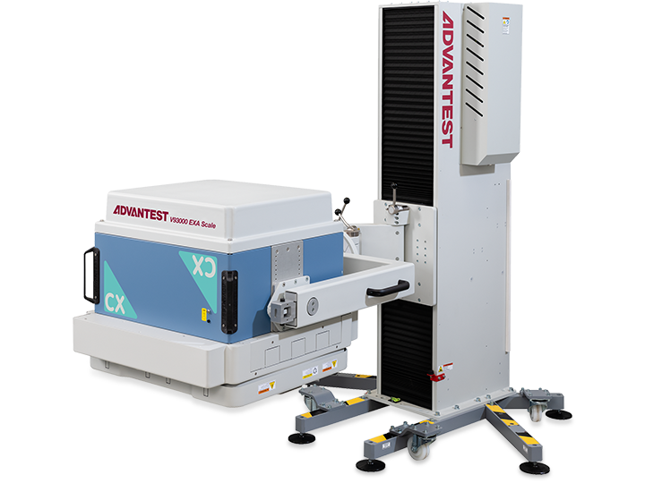
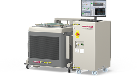
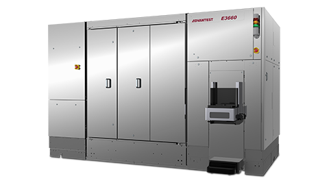
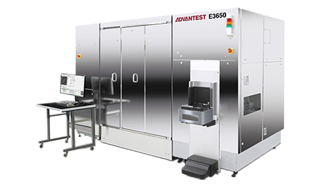
Automated Test Equipment
These systems test semiconductor performance and quality with industry-leading precision and cost efficiency. Robust support for semiconductor design evaluation, volume production ramps, and yield improvement.
-
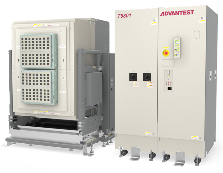
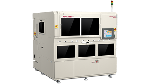
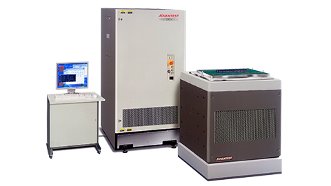
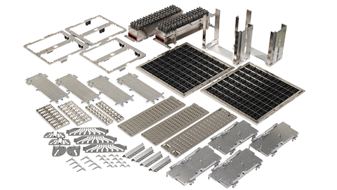
Component Test Systems
These products include test peripherals used with test systems, such as interfaces that connect semiconductor devices with test systems, and handlers that transport semiconductors to the test system. System-level test equipment and software are also included in this category.
-
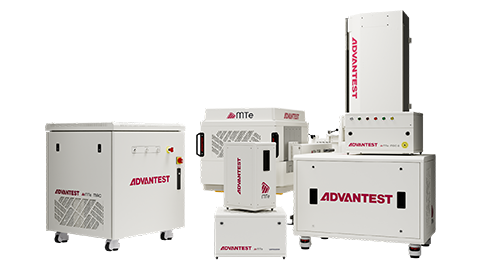
Metrology / SEM
Our SEM products use scanning electron microscope technology to measure and review tiny surface structures such as photomask etching and circuitry on wafers with high precision and stability.
-
Advantest Cloud Solutions™
Our data infrastructure collects data from each semiconductor process and analyzes it using artificial intelligence and machine learning to create real-time optimized solutions that enable productivity improvements across the semiconductor value chain.

-
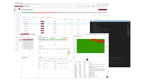
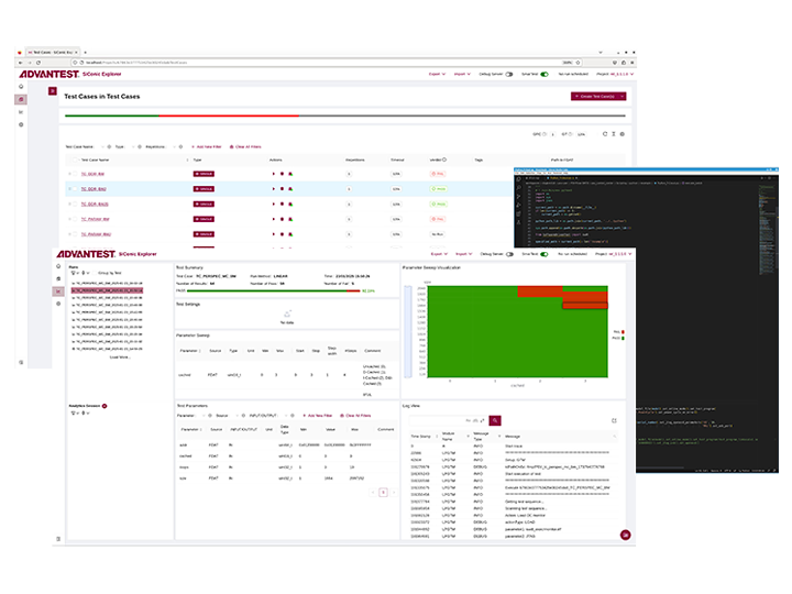
Advantest SiConic™
Advantest’s unified environment to enable a scalable ecosystem and solutions for Automated Silicon Validation.