
Unified Bench Environment Enables DFT Engineers to Execute, Debug and Validate Test Content in V93000-Compatible Workflow
TOKYO, Japan—July 16, 2026—Advantest Corporation (TSE: 6857), a leading provider of semiconductor test solutions, today announced the expansion of its SiConic® ecosystem into a new Design-for-Test (DFT) Engineering environment. Comprising comprehensive bench-level DFT execution and debug functionality, this new environment enables DFT engineers to develop, validate and optimize test content in a production-aligned workflow before deployment to manufacturing.
Advanced-node systems-on-chip (SoCs), AI accelerators and chiplet-based architectures are driving larger pattern volumes and more sophisticated DFT methodologies, contributing to growing semiconductor device complexity. As a result, engineering teams face growing pressure to deliver production-ready test content faster while maintaining confidence in downstream manufacturing test performance.
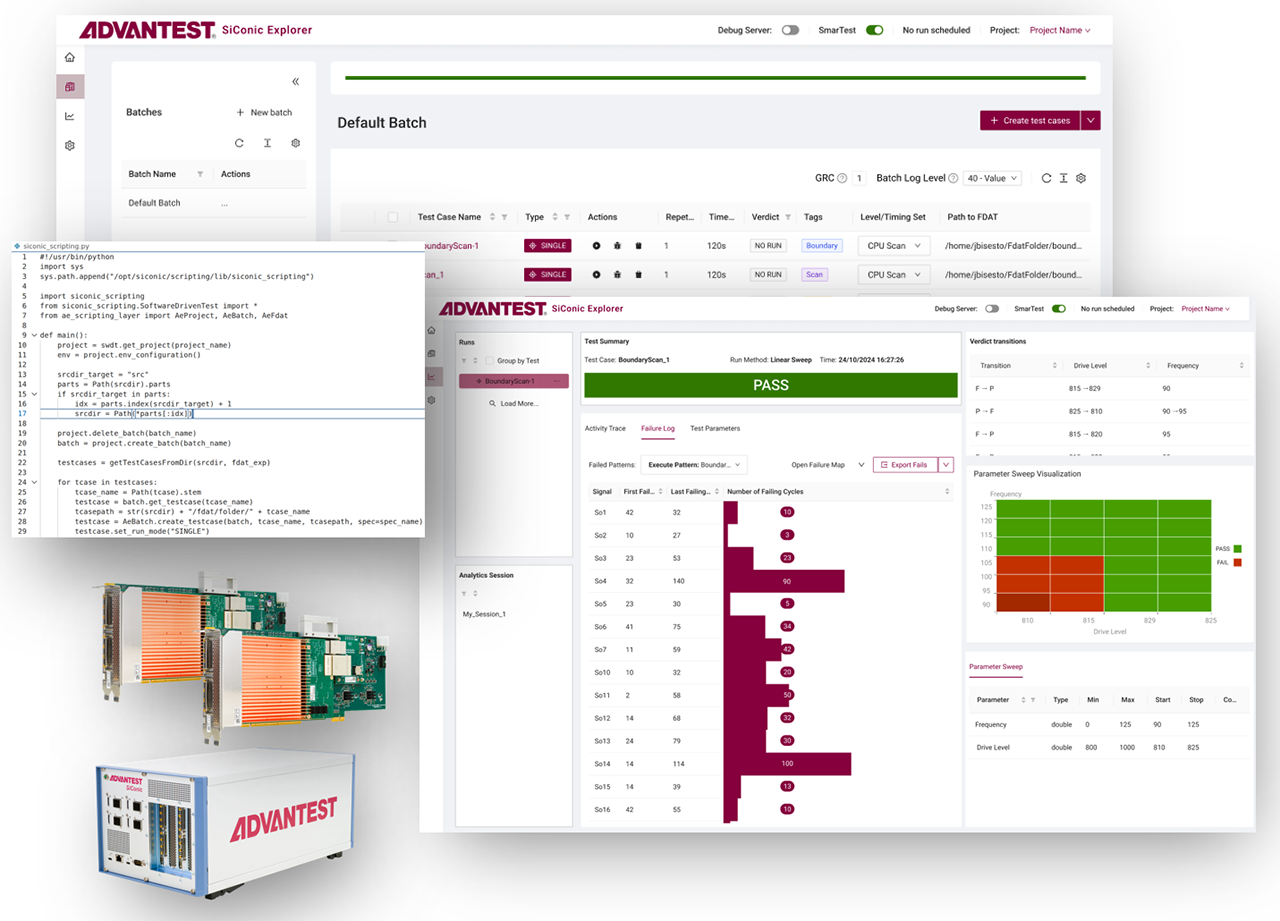
Built on the SiConic platform, the DFT Engineering environment combines the new SiConic D200 digital instrument with SiConic Explorer, SiConic Script, and SiConic Link to provide a unified workflow for DFT pattern execution, debug, automation and validation on the bench. Engineers can generate, execute, iterate and validate DFT content using the same file formats, semantics and execution behavior employed on Advantest's V93000 automated test platform.
Traditionally, DFT engineers have relied on custom-built bench environments with limited correlation to production test systems or have depended on access to production ATE resources for validation. These approaches slow development cycles, create organizational bottlenecks and increase risk during transfer to manufacturing.
By providing a V93000-compatible environment on the bench, SiConic enables DFT engineers to work independently while maintaining alignment with downstream production test workflows. The result is faster iteration, improved collaboration between DFT and test engineering teams, reduced dependence on ATE availability and greater confidence when transferring content to production.
"As complex digital architectures push the boundaries of scale, DFT development has grown far too complex to be treated as an afterthought at the end of the design cycle," said Advantest Chief Technology Officer and Test System Business Group Leader Juergen Serrer. "By extending the actual ATE environment to the bench, SiConic enables DFT teams to validate DFT architecture and timing independently. As needed, design and test engineers can collaborate with DFT engineers to jointly accelerate production ramp in SiConic's unified environment."
Unified DFT Development & Debug Environment
Within the DFT Engineering environment, SiConic Explorer's software-defined workflow provides a DFT-centric user interface for pattern execution, debug and visualization of results, while SiConic Script enables automation and scripting of DFT workflows, allowing engineers to build repeatable debug, sweep, and validation flows. Together, these tools help streamline development and improve productivity across engineering teams.
From a hardware perspective, the solution supports seamless transfer of validated content to the V93000 platform, helping reduce rework and improve first-pass success in production. The new SiConic D200 digital instrument is the key execution enabler, delivering production-aligned digital execution capabilities with data rates of up to 200 Mbps and support for low-jitter clock sources.
The DFT Engineering solution further expands the reach of the SiConic ecosystem, introduced in early 2025, to provide a unified, automated and scalable environment for silicon validation and bench engineering. With this latest addition, SiConic now supports multiple user communities—including design verification, test engineering and DFT engineering—while maintaining tight integration with Advantest's production test platforms. Together, these solutions create a continuous workflow that enables test content to be developed and validated earlier while ensuring smooth transfer into high-volume manufacturing.
Availability
The SiConic DFT Engineering will be available by the end of September 2026. Advantest will showcase the full solution at ITC India, July 19-21, in booth #18.
About Advantest Corporation
Advantest (TSE Prime: 6857) is the leading manufacturer of automatic test and measurement equipment used in the design and production of semiconductor devices such as high-performance compute (HPC), artificial intelligence (AI), automotive, industrial and consumer applications. Founded in Tokyo in 1954, Advantest is a global company with facilities around the world and an international commitment to sustainable practices and social responsibility. Its leading-edge systems and products are integrated into the most advanced semiconductor production lines in the world. The company offers a broad portfolio of test solutions that span the semiconductor value chain, developing advanced test solutions for wafer sort and final test, design verification and silicon validation, and system-level test solutions, as well as test handlers, device interfaces and scanning electron microscopes essential to photomask manufacturing. Advantest also offers data analytics solutions designed to improve semiconductor yield. More information is available at www.advantest.com/en/.
-
Note:All information supplied in this release is correct at the time of publication, but may be subject to change.