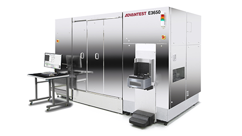
Multidimensional observation and measurement SEM supporting photomasks at sub-10 nm nodes
Amid the progress of multiple-exposure technology, and the development of finer-pitch and more complicated circuits, as well as increases in the number of masks and the number of measurement points on each mask, the size of wiring patterns formed on photomasks needs to be measured and evaluated stably with high precision. Advantest's E3600 series meets the needs of state-of-the-art devices with high measurement repeatability and stable throughput.
The E3650 using Advantest's proprietary electron beam scanning technology, the new tool measures fine pattern dimensions on photomasks with higher precision and stability. The E3650 is the newest entry in the company's E3600 series, which has been widely accepted in the photomask SEM market. It enables measurement throughput to be doubled compared with the existing model, the E3640. E3650's higher throughput enables massive measurement required by more complex patterning and increased number of masks due to multiple patterning. In addition to leading-edge photomasks, the new tool also demonstrates superior performance when measuring EUV masks and master templates for nanoimprint applications.

-
MAM Time, Measurement Precision Greatly Improved (MAM Time : Move Acquire Measure Time)
-
Large Field Measurement
-
Improved Long-Term Stability of CD Measurements
-
DBM (Design Based Metrology) Support
-
3D Observation
-
*To contact us for further details regarding SEM metrology and reviews, please click here.
Click here for Catalogs.
Click here to access the Service & Support page. -
*MVM-SEM is either a registered trademark or a trademark of Advantest Corporation in Japan, the United States and other countries.
- MASK MVM-SEM® E3640
-
MASK MVM-SEM® E3650
- MASK CD-SEM E3660