Corporate Overview
Organizational Profile
(As of April 1, 2026)
| Registered Name | ADVANTEST CORPORATION |
|---|---|
| Head Office | Shin Marunouchi Center Bldg., 1-6-2, Marunouchi, Chiyoda-ku, Tokyo 100-0005 |
| Established | Dec, 1954 |
| Group CEO | Douglas Lefever |
| Capital | 32,363 million yen |
| Stock Exchange Listings | Tokyo Stock Exchange, Prime Market (Securities Code: 6857) |
| Number of Shares Outstanding | 732,000,000 shares |
| Number of employees (excluding temporary employees) |
7,241 (2,209 in Japan and 5,032 overseas. As of March 31, 2026) |
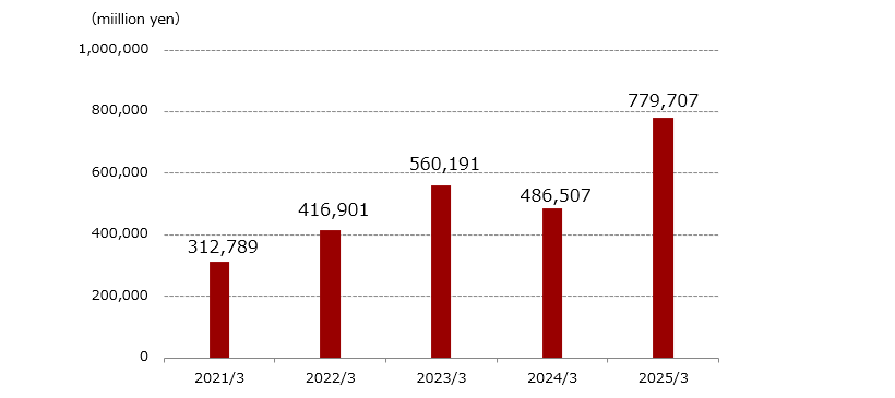
Sales
Change in Net Sale
-
*Financial data are presented in accordance with International Financial Reporting Standards (IFRS).
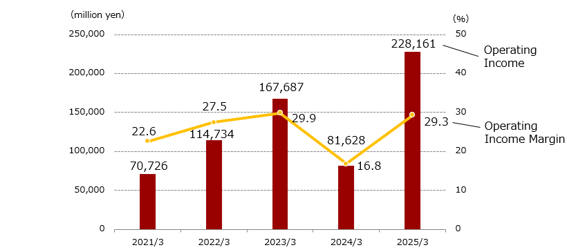
Change in Operating Income/Operating Income Margin
-
*Financial data are presented in accordance with International Financial Reporting Standards (IFRS).
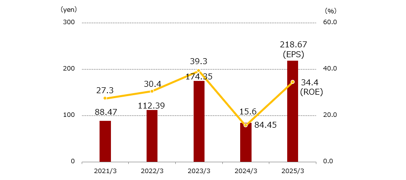
Change in ROE and EPS
-
*ROE: Return on equity ratio of net income attributed to the parent;
EPS: Basic net earnings per share -
*Advantest has issued a 4-for-1 stock split of common stock, effective October 1, 2023.
The above EPS figures are based on the assumption that stock splits were made retroactively.