Fostering Collaboration Across the Supply Chain
As artificial intelligence (AI), high-performance computing (HPC), and edge devices grow in complexity, the need for deeper cross-ecosystem collaboration has never been greater. Advanced packaging techniques, increasing data capacity demands, and evolving reliability standards require new approaches to semiconductor test.
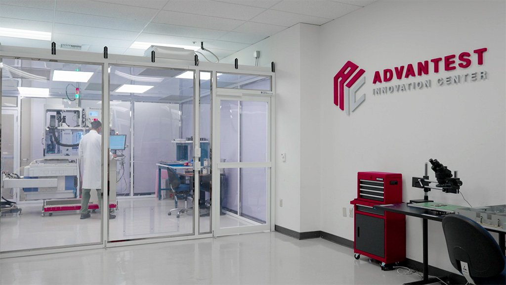
The Advantest Innovation Center was built to meet these challenges.
Featuring state-of-the-art laboratories, clean rooms, advanced test equipment, and the latest test insertions for complex device architectures, the Advantest Innovation Center enables hands-on development of next-generation test solutions. These facilities provide partners with direct access to leading-edge tools and technical expertise—creating an environment where innovation can move faster from concept to implementation.
The Innovation Center also enables the development of innovative, end-to-end workflows that are validated at scale from early design to high-volume manufacturing. This integrated, multi-step approach allows teams to rapidly prototype and refine new methodologies across the entire workflow. At the same time, the unified data architecture created by these workflows supports advanced analytics and AI-driven optimization, unlocking deeper insights across the development lifecycle and enabling smarter, faster decision-making.
With facilities strategically located in the heart of Silicon Valley, Advantest's Innovation Centers will serve as central hubs where partners from across the semiconductor value chain can work side by side with our engineering teams to solve the industry's most pressing challenges.
Partnerships have already been initiated with leading manufacturers and suppliers. If you are interested in finding out more, please contact us through the form below.