Advantest provides products and services that meet our customers' needs by maintaining high product quality and innovating on the technological forefront. Our supplier relationships form the foundation of our business. We aim to grow together with our suppliers through these cooperative relationships.
Supporting Product Safety and Quality
Advantest Group Quality Policy
Customer satisfaction is the ultimate goal of all our activities.
-
(1)We maintain product quality for the entire life cycle of our products and services and satisfy our customers’ requirements throughout the value chain.
-
(2)We fulfill our social responsibility and increase stakeholder satisfaction through continuous improvement of our quality management system to optimize business processes, while complying with all applicable laws and regulations.
-
(3)We provide technologies, products, and services that satisfy customers in a timely manner.
Collaboration with various departments such as marketing, sales, development, quality assurance, manufacturing, and service is essential in ensuring safety and quality throughout the product lifecycle, from production planning to production discontinuation. In this section, we explain how we face the challenges of improving product safety and quality with the aim of enhancing customer satisfaction.
Initiatives to Secure Product Safety and Quality
Advantest adopted the Advantest Product Safety Charter in May 1995 aiming to meet the increasingly high product safety standards and established a company-wide committee to carry out these activities.
In FY2024, we commissioned external specialists to undertake inspections of the safety and durability of 13 major Advantest products. The results indicated that there was no need for further revision of improvement of Advantest's safety specifications.
Advantest operates a 10 m Radio Anechoic Chamber (EMC Center) that complies with the EMC Act required for the sale of products worldwide.
Europe (CE Marking) and South Korea (KC Marking) in particular have strict EMC laws and regulations.
Even in The United States, Advantest takes measures to comply with American EMC laws and regulations (FCC) due to a risk of litigation caused by noise in the surrounding environment when operating products as well as due to customer requirements.
The EMC Center is run by staff who have acquired the ISO17025 international standards regulating the operation of test facilities, in addition to EMC engineers who have been certified under the International Association for Radio, Telecommunications and Electromagnetics (iNARTE), which allow internationally recognized in-house EMC certified testing.
The facilities of the EMC center also put in place an environment that is capable of testing large industrial machinery that is only available in a few places in Japan thanks to equipment that include a turntable with an 8-meter diameter to equip with products, a 3-phase power supply able to supply a total of 148 KVA power capacity that can withstand 10 t, and equipment that can provide water cooling.
It is necessary to keep an eye on the latest legislative trends for each country of origin particularly for EMC laws and regulations. Advantest collects information about EMC laws and regulations by participating in the KEC Electronic Industry Development Center (KEC) working group. We also provide EMC regulatory information to the semiconductor manufacturing industry through the Semiconductor Equipment Association of Japan (SEAJ).
Quality Assurance System
The entire Advantest group (eight countries and 26 sites) is advancing system integration and has acquired the ISO9001 Global Integration Certification as of April 25, 2018, to strengthen global quality management systems. In keeping with our product quality plan where customer satisfaction is the fundamental basis of all our activity, we have established and are operating a company-wide quality management system. We have established an organization to promote the system within the company-wide framework, led by the Quality Assurance Manager under the supervision of the executive management, which maintains and improves quality systems, with the goal of raising customer satisfaction.
As a result, the number of product recalls in FY2024 was zero.
Number of Product Recalls in Past Five Years
Design Review System Aimed at Improving Quality
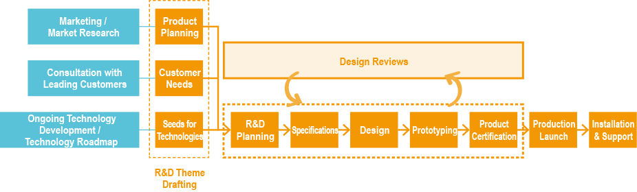
Customers constantly require functionality, performance, and quality in Advantest products. In response, our circuitry has become increasingly larger and complex. Meanwhile, we are also responding to demands for shorter development lead times, a challenge we feel is best addressed by instilling quality at the upstream design phase so that we can detect potential issues early on. Accordingly, we introduced a new design review system in 2008 as a framework for achieving these goals, which we continue to operate while regularly reviewing its effectiveness.
-
At the start of product development, project leaders draw up plans for conducting design reviews, thereby strengthening double-checking of design quality.
-
We changed the system so that not only the relevant staff and the project leader, but also the quality assurance group, identify unresolved issues and prevent follow-up omissions, by enabling the visual identification of issues raised.
-
We also adopted the Design Review Meister System, which involves forming groups of in-house experts for each technical area to participate in the related design reviews. This system increases the rate of problem detection in design reviews, encourages the succession of technologies, and facilitates in-house education. Many positive results have been achieved through these activities.
With the design review system, the rate of defect detection during the design phase has improved, leading to a decrease in setbacks and minimizing development lead time. On the other hand, it has also revealed some cases in which problems that should have been detected by the designer ultimately found their way into the design review or the back-end processes.
Going forward, we will continue to build a design process that achieves higher design quality through careful preliminary checks prior to design reviews.
Activities to Improve Component Quality (SQE Activities)
We are committed to the belief that individual components underpin overall product quality, and therefore the quality of each and every component has to be exceptional. Based on this belief, the Advantest Group engages in SQE (Supplier Quality Engineering) initiatives beginning at the component adoption phase, drawing on the support of our supplier network. SQE initiatives are undertaken with the aim of enlisting a team of experts to bring about improvements to component quality. Accordingly, it is critical that we engage in practices to ensure component quality, particularly given that the number of parts used in our products is roughly equivalent to the 200,000 to 3,000,000 parts that make up an aircraft.
Our SQE initiatives involve the following three practices.
-
Careful selection of components: When given the choice of multiple components with similar performance specifications, we select the best item through a process involving in-house quality analysis and evaluation.
-
Quality improvement through PDCA: We apply PDCA-cycle practices from the component design phase to manufacturing to achieve improvements prior to high-volume production and thereafter.
-
Ensuring that tolerances are maintained in component design: We aim for component design benchmarks determined on the basis of tolerances rather than standard specifications.
In this way, by running SQE activities from the product development
stage, we can reduce problems with components in the manufacturing
process and the risk of component problems reaching the marketplace,
which contributes to greatly reducing the risk of losses. The results
of this approach can be seen in the smooth running of our end users'
processes and in the increased security that our clients enjoy when
using our products.
In addition, by decreasing the number of rejected parts, we decrease
the need for their exchange and disposal, and thus contribute to
reducing the environmental impact.
Availability
Advantest is committed to helping its customers achieve higher levels of productivity by offering them products that guarantee high availability – meaning that they are unlikely to malfunction, and will recover immediately should failure occur. More specifically, availability refers to the ratio of time that a system is operational over a given time, and as such constitutes one of the benchmarks of product integrity. The Advantest Group delivers high availability by working hard to improve MTBF*1 so that systems will operate without malfunction over longer duration of use, while also reducing MTTR*2 so that systems will be more readily serviceable when a malfunction does occur.
-
*1To improve MTBF: MTBF: Mean Time Between Failure
-
*2To reduce MTTR: MTTR: Mean Time To Repair
Initiatives Aimed at Improving Software Quality
Advantest continues to implement initiatives aimed at improving software quality. Software for test systems, handlers and other such systems shipped by Advantest first goes through a process that involves quality verification by the Quality Assurance Group. The specification sheet, a parallel product of development, is examined by the Quality Assurance Group in real time and feedback is given, which helps to ensure quality at upstream stages of development. The examination is implemented before development is completed, and after it has been confirmed that quality standards have been met, products are shipped.
Advantest promotes the incorporation of Automotive SPICE*1 into the development process in order to ensure the quality of embedded automotive software. In 2021, we obtained Automotive SPICE Level 1 certification for the V93000 system software SmarTest. We are also working to obtain Automotive SPICE Level 2 certification for T2000 system software. These initiatives help to bring about the timely delivery of even better products.
-
*1Stands for "Automotive Software Process Improvement and Capability Determination", which is an automotive industry standard software development process model
Use of Customer Feedback to Improve Product Quality
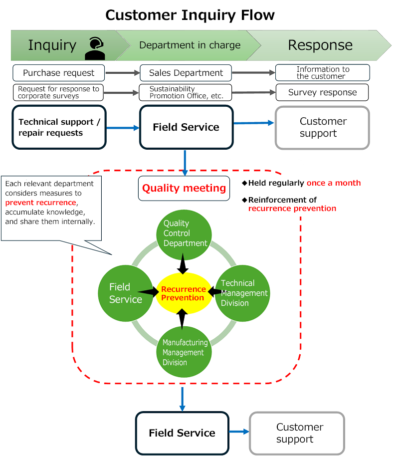
We have established a system to respond quickly and accurately to the diverse inquiries we receive from our customers.
Inquiries are categorized into three main types: "purchase requests," "requests for responses to corporate surveys," and "technical questions," and are promptly routed to the appropriate department. Inquiries regarding the introduction of products and services are handled by the sales department, while matters related to environmental and social responsibility are handled by the Sustainability Promotion Office and other departments. In the event that technical questions or on-site support is required, the Field Service Department, which has expertise in the field, will respond to the customer's request. Each department provides not only answers to customers' requests but also offers optimal proposals and arrangements as necessary to provide ongoing support. In this manner, we aim to build a relationship of trust with our customers and form long-term partnerships. At quality meetings held regularly by related divisions, the details of responses and knowledge gained in the field are shared among members and utilized in the consideration and implementation of measures to prevent recurrence.
In this way, we are working to continuously improve service quality and customer satisfaction by directly incorporating feedback from the field into our quality improvement efforts.
Efforts to Improve Customer Satisfaction
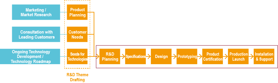
To improve customer satisfaction, we strive to develop and manufacture products that satisfy customers’ needs, keeping abreast of market trends. In order to develop products that exceed customer expectation, we conduct appropriate design reviews in the process of product development including various departments; not only Manufacturing Division and Quality Assurance Division but also Sales Group, Field Service Group, Marketing Division, and other related departments who directly communicate with our customers.
In addition, we have set two KPIs in our Sustainability Action Plan with the aim of contributing to solving customer issues.
Basic Policy for Improving Customer Satisfaction
-
(1)We maintain product quality for the entire life cycle of our products and services and satisfy our customers’ requirements throughout the value chain.
-
(2)We fulfill our social responsibility and increase stakeholder satisfaction through continuous improvement of our quality management system to optimize business processes, while complying with all applicable laws and regulations.
-
(3)We provide technologies, products, and services that satisfy customers in a timely manner.
By sharing the above product quality policy throughout the Group, we strive to offer products that provide not only superior performance but also superior environmental friendliness and safety. We are committed to keeping our customers satisfied at every stage, from design and manufacturing to sales and service, by providing an ever higher level of guaranteed quality, top-notch service, and support on a global scale.
Sales and Marketing Practices to Ensure Higher Customer Satisfaction
Global operations in sales and marketing also require cross-functional and cross-regional teamwork.
Today, the process from semiconductor design to manufacturing is handled by both design-only companies, known as fabless, and many companies that are contracted to manufacture and test semiconductors, known as foundries/OSATs.
Many of our test systems are installed at those contractors, but testing begins at the upstream design evaluation stage. The tester business requires not only discussions with foundries/OSATs, but also coordination of fabless intentions and conclusion of business negotiations.
In addition, the semiconductor supply chain spans globally, with fabless companies in North America and foundries/OSATs based in Asia, and in many cases, the companies are geographically separated. We have a cross-regional team of account sales, marketing, systems engineers, field service, and even R&D working with our customers. We integrate customer needs, semiconductor market and test technology trends, and our solution portfolio to propose solutions that satisfy both fabless and foundry/OSAT requirements as much as possible. This global, seamless, and attentive support helps strengthen our partnership with our customers.
Sales and Marketing Activities to Improve Customer Satisfaction
Not only do we provide test solutions, but also keep our customers up-to-date on the latest technology and product information related to the market so as to stay committed in supporting our customers' technical innovations. Due to the impact of COVID-19, we held our conventional face-to-face exhibitions and customer events online; however, beginning in 2022, we are resuming in-person events while taking vigilant measures to prevent the spread of infection. In June 2024, we successfully held the VOICE - Advantest Developer Conference in San Diego, California, USA. VOICE is run by a committee made up of Advantest and voluntary customers, serving as an international community where users and strategic partners related to our product portfolio gather and grow together. The conference is also a place for participants to deepen their insights and build lasting relationships by discussing the efficiency and productivity of semiconductor testing and learning about the latest technology trends and applications.
Promoting Customer Support
The Advantest Group has established its basic policy for customer
support with the aim of realizing the globally-oriented restructuring
of the Group's service businesses.
Our basic policy is outlined as follows.
Basic policy for customer support
-
We will propose total solutions in the form of support packages designed to deliver maximum efficiency to our customers in their device measurement operations.
-
We will propose unified service support matching the customer's business model from development to the mass production environment.
-
We will respond to customer demands by proposing service support packages that encompass total solutions.
-
We will always take the customer's point of view and draw on our global organization in offering solutions.
-
Our premium services and customer support will not only be efficient, but will also take the environment and safety into consideration.
-
We will offer high-value-added professional services.
-
We will strive to maintain our zero-accident record by thoroughly observing safety standards in field service provision and elsewhere.
Better Customer Support with a Global Focus
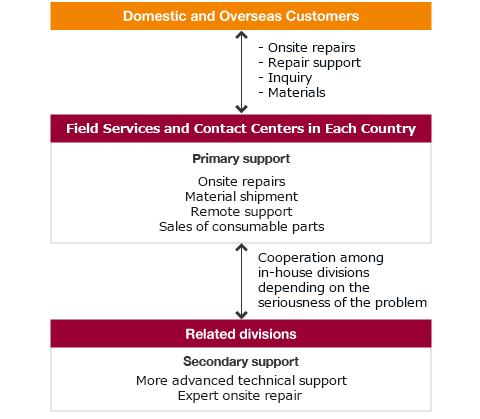
Advantest is building a global support framework capable of responding effectively to a variety of customer support requests and inquiries from customers. While responding to routine inquires through customer contact centers in each country, as well as by telephone and e-mail, we are also implementing primary support consisting of technical service and onsite repairs by field service engineers.
We place expert global support teams in product development bases to carry out secondary support, allowing us to respond appropriately based on the content and degrees of difficulty of customer support. This way, we are working to improve customer satisfaction while building relationships of trust with customers through a system that can provide high-quality services.
We have developed a global supply-chain network covering customer operations ranging from their development bases to mass production facilities. Moreover, we also operate a supply-chain control mechanism through which replacement equipment and parts at service centers in each country are monitored to determine inventory needs at respective locations worldwide.
We continue to run an engineer exchange program between overseas subsidiaries and our secondary support division, which helps field service engineers improve their professional skills and raises the quality of our support. This two- to three-year human resource development program aims to sharpen engineers' technical skills, develop cross-cultural competencies, and raise foreign language and communication proficiencies.
In the mass production facilities of customers, we offer on-request expert engineering consulting and solutions regarding productivity issues and issues related to apparent expectations. We aim to increase customer value through collaborative creation with our customers for issues related to latent expectations that customers themselves are unaware of, by incorporating methods such as ethnography and service science to explore the issues.
Customers' Contribution to 3R
Advantest is actively involved in 3R initiatives for our product through Advantest Pre-Owned Solutions Corporation, our subsidiary.
When customers no longer use our products, we purchase them instead of simply disposing them, ultimately contributing to "reduce". We promote the "reuse" of our products by reselling the equipment we purchase to other customers who have been using them for a long time, or by providing them with parts.
If there is no demand for the equipment or parts, we sort the equipment we take back to the resource levels and "recycle" them.
We have defined our approach to the used products as “remarketing" and are committed to working together with our customers to solve their issues by providing a single point of contact and integrated services.
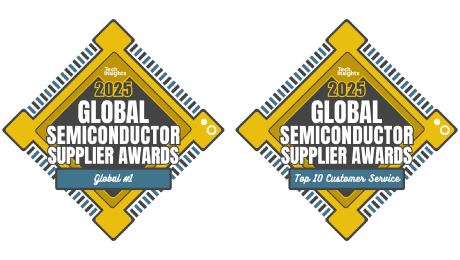
Advantest Named THE BEST Supplier of Chip Making Equipment and #1 ATE Supplier for 6th Consecutive Year by TechInsights
Advantest aims to grasp customer needs accurately and strives to provide customers with high-performance, high-quality total test solutions in a timely manner.
We make efforts to gain a better understanding of our customers' needs through information that we acquire from our daily business activities, and also through yearly participation in the customer satisfaction survey conducted by TechInsights, a company renowned for its semiconductor market research. These efforts have been incorporated into our Sustainability Action Plan.
In the 2025 Customer Satisfaction Survey, Advantest captured the No.1 spot of global semiconductor companies for the sixth consecutive year. The company was also named on the Top 10 Customer Service (previously known as 10 BEST Suppliers) list of large suppliers of test equipment for the 37th consecutive year. Advantest achieved high customer ratings in the areas of Partnering, Recommended Supplier, Trust in Supplier, Technical Leadership, Commitment, Engineering Support, and Application Support and was the only ATE supplier to receive a five-star rating again this year.
Some reviews from our customers
Related News
Innovation Initiatives
With the aim of "enabling leading-edge technologies," Advantest conducts research and development of fundamental technologies and products that will lead to greater value creation in the area of measurement technologies that support the semiconductor industry, the electronics industry, and the information and telecommunications industry. The results of these R&D activities contribute to the evolution of the semiconductor value chain on which our business is based on. In addition, we contribute to the realization of a safe, secure, and comfortable society by promoting the widespread use and social implementation of semiconductors with high performance and economic efficiency. Since R&D activities are a direct source of not only our own growth, but also of expanding our contribution to society, we have positioned R&D as an area of investment of utmost importance, and have invested a large amount of capital over the long term.
Summary of Innovation Initiatives
We wish to continue to be a company that provides high-value, world-class, state-of-the-art semiconductor test technology to all of our semiconductor customers. Our customers include many of the world's technology leaders, including the world's leading semiconductor manufacturers and IT companies, and their future success leads to the success of Advantest. On the other hand, in order to continue to create products and solutions that meet the high expectations of these customers, we must overcome a number of technological hurdles, which requires long-term, sustained, large-scale R&D management with a timeframe of 5 to 10 years. Our R&D management is based on a medium- to long-term roadmap, which is formulated based on the future technology needs and investment forecasts gathered through close communication with our customers, as well as market research on future technology trends and demand forecasts in the semiconductor-related market.
We are also engaged in developing new measurement solutions for medical devices and other applications outside the semiconductor value chain that leverage our electronic and optical measurement technologies.
Major basic technology developments in the most recent fiscal year
-
Development of optical semiconductor devices, light sources, and optical integrated circuits for optical measurement and collective optoelectronic device test systems
-
Development of sensor technology, algorithm technology, and application technology for ultra-sensitive magnetic measurement
-
Elemental technologies such as pin electronics, pattern and timing generation, and DC test resources for semiconductor and component test systems
-
Development of compound semiconductors such as low-distortion devices and high-speed, high-frequency devices for use in semiconductor and component test systems
-
Development of technologies that enable testing of next-generation protocols and optical signal interfaces, including multi-level transmission
-
Development of calibration methods capable of simultaneously adjusting the timing and waveform quality of ultra-high-speed signals with multiple pins
-
Development of data linkage and analysis methods throughout the semiconductor supply chain, from the design process to the test process
Expansion of Direct Contributions to the Realization of a Sustainable Society through Innovation
At Advantest, all products undergo a product environmental assessment. In addition, we are committed to incorporating the improvement of environmental performance, such as power consumption efficiency, into our R&D process for new products, in view of contributing to a decarbonized society. Our contribution to the realization of a sustainable society is therefore integrated with our business activities.
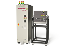
Test solutions appealing to diverse customer needs
V93000 Series
The requirements of today’s industry for even higher speeds, performance and pin counts means that test systems must offer greater functionality while maintaining low cost of test. With its scalable platform architecture, the V93000 tests a wide range of devices, from low cost IoT to high end, such as advanced automotive devices or highly integrated multicore processors. It also requires not only innovative technology, but also a system architecture with a long use-life, high scalability, and high investment efficiency.
The V93000 tests a wide range of devices, from low cost IoT to high end, such as advanced automotive devices or highly integrated multicore processors. Staying focused on the single scalable platform strategy, the V93000 is widely accepted at the leading IDMs, foundries and design houses. Outsourcing IDMs and fabless companies find V93000 test capacity installed in all leading OSATs worldwide.
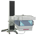
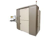
Memory Test Systems
Since the 1990s, Advantest has continued to provide close technical support to customers developing cutting-edge technologies, and over the past 30 years, we have accumulated a wealth of experience and solid technical expertise in memory testing by seamlessly following the technological evolution of memory semiconductors. We have consistently established our position as a de facto standard in memory testing by enabling faster time-to-market for optimal test solutions, especially for high-end memory.
Memory Test System
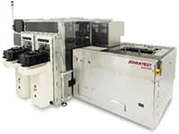
Test Handlers
AI/HPC ICs require 2.5D/3D advanced packaging technologies to provide the high computing power necessary to generate, train and run data-intensive AI models. These ICs generate massive heat due to their high compute power, creating unique testing challenges. The new Advantest test handlers are designed to address these challenges and help contribute to the AI/HPC market growth.
Die-level Handler
Advantest Cloud Solutions™ (ACS)
With the aim of expanding and growing corporate value, Advantest is extending its solutions by enhancing test solutions and introducing new technologies. As an example, Advantest has been promoting Advantest Cloud Solutions™ (ACS), which integrates data generated through customers' semiconductor manufacturing processes with semiconductor testing data, which is then analyzed to generate new value.
The Advantest Cloud Solutions™ (ACS) ecosystem helps customers accomplish intelligent data-driven workflows. The ACS open solution ecosystem, a family of cloud-based products and services, is based on a single scalable data platform, which enables customers to develop or procure market-leading solutions from Advantest and its partners. Using these real-time machine learning, market-leading solutions, customers can automate turning insights into production actions in an easy-to-use and accessible way across the entire semiconductor value chain.
System Level Test Systems
As a new test solution, Advantest is developing products that support system level testing to guarantee the performance of the final product. While System Level and Burn-In tests are not new methodologies, both are gaining more momentum particularly for production test.
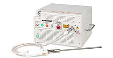
Fluorescence Detection System
The E5620During laparoscopic surgery, the fluorescence detection system, Lumifinder™ irradiates the observation site, to which a contrast agent (indocyanine green) has been administered in advance, with a near-infrared laser beam. The intensity of the resulting fluorescence is displayed numerically and graphically, providing quantitative data for better real-time decision-making. Fluorescence intensity spectrum waveforms and changes in intensity can also be observed. In addition, the Lumifinder™ can connect to the laparoscopic camera video signal, enabling medical staff to observe fluorescence while checking the laser irradiation position visually.
The Lumifinder™ is the first medical device Advantest has released in its approximately 70-year history (medical device approval number: 30500BZX00031000). It has been introduced at select medical institutions starting in 2023, and began offering the product on a lease basis to general medical institutions in Japan from April 2024. Please note that at present, it can only be used within Japan.
Fluorescence Detection System
External Collaboration
Advantest aims to contribute not only to semiconductor testing but also to the entire semiconductor value chain by promoting innovation through industry-academia collaborations and other external collaborations, as well as through human capital development initiatives.
In addition to the above, we have established "The Advantest D2T Research Division" at the Tokyo University Graduate School of Engineering, with the aim of developing specialists in test design and supporting research activities for SoC (System on Chip) design.
Together with the University of Tokyo, Advantest has begun working on research and development of new, advanced system technologies from April 1, 2023 in the Research Association for Advanced System (abbreviated as RaaS, hereafter referred to as RaaS*1). The members of the cooperative, the University of Tokyo, Advantest, Toppan Inc., Hitachi Ltd., Mirise Technologies Corporation, and Japan’s RIKEN Scientific Research Institute, etc., will work together to do R&D on a next-generation leading-edge semiconductor development platform that can be shared among the members.
-
*1RaaS
An acronym of the Research Association for Advanced Systems. It advocates the provision of semiconductors not as components (products) but as core system knowledge (services), and reads “Raas”. It also stands for “research as a service".
URL: https://raas-cip.org/
Intellectual Property Initiatives
Basic Stance Toward Intellectual Property
The basic principles of Advantest's intellectual property management are compliance with intellectual property laws and regulations and respect for the intellectual property of third parties.
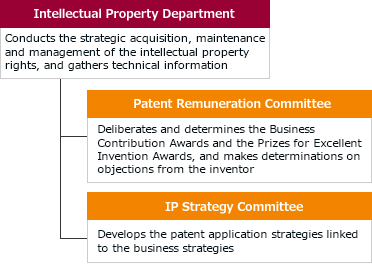
Organization of Intellectual Property Management
Advantest has established the following intellectual property management systems, and carries out appropriate intellectual property management in cooperation with business units in Japan, Germany and the U.S., which are our main development bases and affiliates in each country.
The Intellectual Property Department conducts online meetings as necessary with intellectual property managers in Germany, the U.S., Singapore and China, and holds IP Strategic meetings twice a year with the IP Strategic Committee members to promote intellectual property activities in accordance with business unit, research and management plans.
The Patent Remuneration Committee consists of members in Japan, Germany and the U.S., and the members meet to determine patent remuneration payments as compensation or incentives to inventors.
The IP Strategic Committee is selected from among the various business units and subsidiaries in Japan, Germany and the U.S., and formulates IP strategies linked to the business strategies.
Intellectual Property Strategies
The strength of Advantest is our state-of-the-art technological capabilities. Therefore, we believe protecting our intellectual property as the source of our competitiveness vital to persist as an enterprise. Therefore, Advantest is unceasing to build a strategic intellectual property portfolio from a Group-wide perspective, in close collaboration not only with the R&D department, but also with the marketing department and management.
Intellectual Property Education
Advantest is actively engaged in in-house education striving to raise each employee's awareness of intellectual property.
In fiscal 2024, training was provided to newly appointed managers on compliance issues related to intellectual property and the handling of intellectual property at Advantest. In addition, intellectual property education via e-learning was conducted for all employees of the Advantest Group in Japan and overseas to improve their intellectual property literacy.
As part of our Efforts Toward Social Contribution, we held classes and workshops for elementary school students to promote IP creation education. Please refer to "Examples of Social Contribution Activities" for details.
Disputes and Litigation Relating to Intellectual Property
As of March 31, 2025 there were no such disputes.
Responsible Sourcing
Cooperative relations with our business partners are the foundation of all our businesses. We value communication with our business partners, and maintain fair business dealings with them based on related laws and regulations.