MASK MVM-SEM® E3600 series
Multi Vision Metrology Scanning Electron Microscope
Together with the miniaturization of semiconductors, high-accurate and stable measurement and evaluation is needed for circuit patterns such as mask patterns and holes. Advantest's E3600 series are used by a wide variety of companies, from semiconductor manufacturers to photomask makers to device and materials producers.
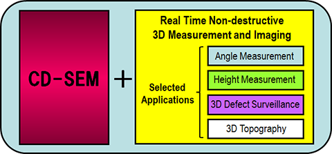
In addition to its high-functionality CD-SEM features, the E3630 makes 3D imaging and measurement at the nanometer level, in real time and in a non-destructive way, possible. The E3630 significantly contributes to reducing TAT in R&D and production for many processes that require high-precision and/or 3D analysis.
-
High-speed, high-precision pattern measurement at the nm level
-
3D topography imaging
-
Imaging of sample surface irregularities
-
Automatic critical dimension measurement of complex circuit patterns
-
Measurement and imaging of MEMS, nano-imprint lithography, and various insulating materials
-
*To contact us for further details regarding SEM metrology and reviews, please click here.
Click here for Catalogs.
Click here to access the Service & Support page. -
*MVM-SEM is either a registered trademark or a trademark of Advantest Corporation in Japan, the United States and other countries.