1Xnm Process Coverage
Ongoing semiconductor process shrinks are driving new demand for stable, highly precise measurement of pattern dimensions for photomask and wafer production. The E3640 satisfies these requirements with industry-leading precision measurement capabilities and upgraded functionality that enhances mask R&D and production efficiency.
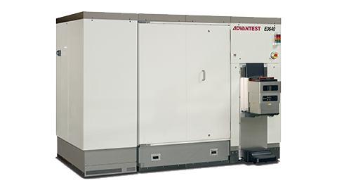
Advantest's new E3640 Multi Vision Metrology SEM tool supports pattern measurement for photomasks and other patterned media at dimensions as small as 1Xnm. A new entry in Advantest's widely-adopted E3600 Series of SEM systems, the E3640 delivers significantly improved measurement accuracy and higher throughput. Its industry-best pattern measurement capability supports the coming shift to the 1Xnm node for semiconductor volume production. In addition to photomasks for standard semiconductor lithography, the E3640 also offers enhanced metrology performance for EUV masks and NIL templates.